Get Free Admission Guidance
Share your details and our counselors will call you.
PhD in Materials and Devices: Eligibility, Fees & Admission
INTRODUCTION
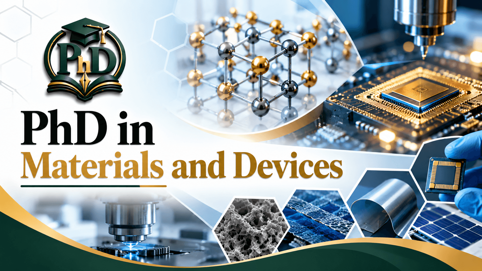
A PhD in Materials and Devices is a research-based doctoral programme focused on advanced materials, semiconductor technologies, electronic devices, nanotechnology, energy materials and related research areas. Since the exact programme title varies across institutions, similar research may be offered through Materials Science, Materials Engineering, Physics, Electrical Engineering, Electronics or Nanotechnology departments.
Research work is mostly carried out in this course and the research scholars can make use of material synthesis, material characterization, device fabrication, microscopy, spectroscopy, computation techniques, simulation, electrical and optical measurement techniques, etc., for researching about the materials and devices. The research areas might include semiconductor materials, nanomaterials, thin films, electronic devices, optoelectronic devices, energy storage and conversion materials, sensors, quantum materials, nanoelectronics, flexible electronics, and more.
The course duration in general is three years along with the coursework and the exact duration depends upon the type of the research project, university guidelines and progress of the research scholar. The applicant has to obtain a Master's degree or some other postgraduate degree from an approved institution according to the UGC and the respective institution. In general, the minimum educational qualification will be the postgraduate one, along with some relaxations and conditions set by the institution.
Admission criteria for a PhD program vary widely according to the admitting institution. Some institutions take into account the NET, CSIR-NET, GATE, JEST or any other recognized qualification, whereas some others hold entrance examinations for the PhD programs and personal interview/ research discussion. On the institutional level, the admission process may consider the area of research, educational qualification, aptitude in research, performance in the entrance test and availability of a suitable supervisor and facilities for research.
PhD in Materials and Devices: What Is It About?
A PhD in Materials and Devices is an advanced study course centered around materials and the devices or technologies that are developed with them. The nature of a doctorate differs to that of a Masters where the focus is upon achieving a general understanding of an academic field. The task of a research scholar is to define a problem, to review the literature, to develop an appropriate research methodology, to perform experiments or simulations and to add new knowledge and findings related to the area of science.
Depending on the university and research groups, the study of materials and devices can cover a number of areas such as:
PhD in Materials and Devices at a Glance
| Degree | Doctor of Philosophy (PhD) |
| Duration | Minimum 3 years including coursework |
| Eligibility | Relevant Master's degree / applicable bachelor's route |
| Primary Fields | Materials Science, Materials Engineering, Device Technology |
| Entrance Exams | NET/CSIR-NET/GATE/Institute Test, depending on institute |
| Study Mode | Full-time; part-time where offered |
| Research Areas | Semiconductor materials, nanomaterials, devices, sensors, energy materials |
| Admission Process | Application → Shortlisting/Entrance → Interview → Selection |
| Final Outcome | Doctoral thesis and viva voce |
Is PhD in Materials and Devices Worth It?
The PhD in Materials and Devices may be a perfect fit for those who want to become involved in research in the field of advanced materials, semiconductor devices, devices, nanotechnology, energy systems, and academic career. The program may lead to work in universities, research institutions, semiconductor industry, electronics research and development, energy technology, and materials industries.
Nevertheless, it should be noted that the degree may be valuable depending on the research field, level of the supervisor, laboratory facilities, publications, skills, and career goals.
Why Pursue a PhD in Materials and Devices?
1. Conduct Advanced Materials Research
A PhD allows candidates to study a specific materials or device problem in depth. Research may involve: Semiconductor materials, Nanomaterials, Electronic materials, Thin films, Energy materials, Functional materials, Magnetic materials.
2. Develop Specialised Expertise
Materials and device research covers a wide range of technologies. Doctoral research allows a research scholar to develop specialised knowledge in a particular area. Possible specialisations include: Semiconductor devices, Electronic materials, Nanoelectronics, Thin-film devices, Sensors, Optoelectronics, Energy materials, Flexible electronics, Photovoltaic devices.
3. Work on Emerging Technologies
Materials and devices are important in many emerging technologies. Doctoral research can explore areas such as: 2D materials, Advanced semiconductor devices, Quantum materials, Flexible electronics, Wearable devices, Energy-storage technologies, Artificial intelligence hardware, Advanced sensors, Nanoelectronic devices.
4. Build an Academic and Research Career
A PhD can support careers in universities, research institutes and specialised R&D organisations. During doctoral study, research scholars can develop experience in: Research publications, Laboratory research, Technical presentations, Conference participation, Material characterisation, Device fabrication, Research collaborations.
5. Work on Materials and Device Problems
Research in this field can contribute to technologies used in: Semiconductor electronics, Solar energy, Energy storage, Healthcare devices, Sensors, Telecommunications, Automotive electronics, Industrial systems, Consumer electronics.
6. Work Across Multiple Disciplines
Materials and device research often combines: Physics, Chemistry, Materials science, Electrical engineering, Electronics, Nanotechnology, Mechanical engineering, Chemical engineering, Computer science.
PhD in Materials and Devices Duration
The UGC framework specifies a minimum three years of PhD including the course work. The maximum time limit and the provisions of its extension beyond the stipulated period will be decided by the relevant acts and the PhD rules of the university.
A typical doctoral journey may include:
| Stage | Approximate Period |
|---|---|
| Admission and Registration | Initial stage |
| Coursework | First phase |
| Literature Review | Early research |
| Research Proposal | After initial coursework/research preparation |
| Material Synthesis / Device Development | Main research stage |
| Data Collection | Main research stage |
| Data Analysis | Main research stage |
| Thesis Writing | Final stage |
| Thesis Submission and Viva | Completion stage |
The actual duration should therefore be checked in the regulations of the institute offering the programme.
PhD in Materials and Devices Eligibility Criteria
Eligibility criteria may vary across institutions, but the UGC PhD framework provides a broad academic framework for doctoral admission.
As per the UGC 2022 Regulations, candidates should meet one of the following academic qualifications to be eligible:
- Postgraduate degree, one year or two semesters of study after completing a four-year or eight-semester bachelor's degree program,
- Two-year or four-semester Master's degree after completing a three-year bachelor's degree,
- An equivalent qualification as may be prescribed by the relevant statutory or regulatory authority.
The specified Master's route generally requires at least 55% marks or an equivalent grade. The regulations also provide a 5% relaxation for specified categories, subject to the applicable rules.
Universities may additionally require the previous qualification to be in a relevant field such as:
The required academic background can be dependent upon the proposed research area. For instance, a candidate applying for semiconductor device research would be required to have a background in electronics, electrical engineering, physics, materials science or a related subject.
Generally, eligibility requires a relevant Master's degree or equivalent qualification as specified under the applicable UGC and the university regulations. Under the applicable UGC framework, candidates entering through the relevant four-year bachelor's route may require 75% or equivalent, subject to applicable relaxations and the admission rules of the institution.
PhD in Materials and Devices Entrance Exam And Admission Route
There is no single entrance examination that is mandatory for every PhD in Materials and Devices in India.
Universities may follow one or more of the following routes:
- UGC-NET / JRF: UGC-NET could be essential for PhD eligibility and/or fellowship depending on the subject category and institution.
- CSIR-UGC NET / JRF: CSIR-UGC NET could be for candidates with science backgrounds, contingent upon the subject, area of research and admission rules of the institution.
- GATE: GATE scores may be accepted for consideration by specific institutes and admission categories, specifically for engineering and technology related doctoral programmes. But GATE requirements may vary between universities and departments.
- University-Level PhD Entrance Test: Institutions may conduct their own: Written examination, Aptitude test, Subject-specific test, Research aptitude test. The examination may cover materials science, physics, chemistry, engineering or other subjects related to the proposed research area.
- Interview / Research Discussion: Shortlisted candidates may be assessed on: Research interests, Subject knowledge, Problem-solving ability, Academic background, Research proposal, Previous project or dissertation, Research motivation, Understanding of the proposed research area.
Common Admission Routes for PhD in Materials and Devices
Route 1: National-level qualification
UGC-NET / CSIR-NET / GATE / JRF or another recognised national-level qualification → University application → Shortlisting according to institutional rules → Interview / research interaction → Final selection
Route 2: University entrance examination
University application → PhD entrance examination → Research-oriented interview → Final selection
The UGC PhD framework allows universities to hold their own entrance examinations, if they so wish. The relevant entrance-test structure and interview requirements should be checked in the university's current admission notification.
Is NET or GATE compulsory?
It is not mandatory for every PhD in Materials and Devices.
In some cases the necessity depends on the university, department, background, category of admission and area of research. Some universities may consider GATE or NET/JRF and some may have their own entrance exam and selection process.
Therefore, candidates should not assume that "NET or GATE is always required" or "NET or GATE is never needed." The latest university admission notification should always be checked before applying.
PhD in Materials and Devices Admission Process
- Step 1: Select the Research Area – Candidates should identify a research area based on academic background, research interests, laboratory facilities and faculty expertise. Possible areas include: Semiconductor materials, Nanomaterials, Electronic materials, Thin films, Semiconductor devices, Sensors, Energy materials, Optoelectronic devices, Flexible electronics, Quantum materials.
- Step 2: Check Eligibility – The university's latest admission notification should be checked for: Required degree, Minimum marks, Accepted academic background, GATE/NET requirements, Entrance test, Research area, Supervisor availability, Additional requirements.
- Step 3: Submit the Application – Candidates generally apply through the official institute portal and submit academic documents, certificates, mark sheets, qualifying examination details and other required documents.
- Step 4: Entrance Test or Shortlisting – Shortlisting may consider: GATE or another recognised qualification, Institute-level entrance test, Academic performance, Research background, Relevant technical knowledge, Research interests, Faculty or research-area alignment.
- Step 5: Research Interview – The interview can cover: Materials science fundamentals, Physics and chemistry concepts, Semiconductor materials, Device fundamentals, Research methodology, Previous project or dissertation, Proposed research interest, Technical fundamentals.
- Step 6: Final Selection – Candidates fulfilling the selection criteria of the institute are eligible to get admission offers. The registration and doctoral studies commences as per the PhD regulations of the institute.
Students planning to pursue a PhD can also check the guide on PhD Admission in India to understand the admission process, eligibility criteria and important requirements.
Documents Required for PhD in Materials and Devices
Possible documents include:
The exact document requirements can vary between universities.
PhD in Materials and Devices Fees
The fee structure of PhD in Materials and Devices varies depending on the university, programme structure, student category and other academic charges.
Government and publicly funded institutions may have comparatively lower academic fees, while private universities can have higher tuition and other charges.
Common fee components can include:
| Institution Type | Approx. Annual Academic Fee |
|---|---|
| Central / public universities | ₹10,000–₹50,000 |
| State public universities | ₹15,000–₹75,000 |
| IITs / centrally funded technical institutes | ₹25,000–₹80,000+ |
| Deemed / private universities | ₹80,000–₹2.5 lakh+ |
| Specialised materials / research institutions | ₹1 lakh–₹3 lakh+ |
| Additional research-related expenses | Varies by project |
The above figures are approximate ranges, and not a set national fee structure. They are offered only as a general guide since actual fees may vary substantially from one institution, category and academic year to another. Please refer to the most recent official notification of fees pertinent to candidate application before submitting it.
PhD in Materials and Devices Syllabus / Coursework
Some of the common courses are listed below:
Research Methodology
Materials Science
Electronic Materials
Device Technology
Advanced Materials and Devices
Simulation and Characterisation Tools
Depending on the research area, scholars may work with:
Research and Publication Ethics
PhD in Materials and Devices Research Areas
1. Semiconductor Materials and Devices
Research can be carried out on semiconductor materials, device design, fabrication, modelling and performance analysis.
2. Electronic Materials
Research may focus on materials used in: Transistors, Memory devices, Displays, Sensors, Electronic circuits.
3. Nanomaterials and Nanoelectronics
The research can be about nanoscale materials, low-dimensional systems, nanostructures and advanced electronic devices.
4. Thin Films and Coatings
Research may focus on: Thin-film deposition, Thin-film transistors, Functional coatings, Optical films, Electronic films.
5. Optoelectronic Materials and Devices
Research may be about: Photodetectors, LEDs, Solar cells, Optical sensors, Photonic devices.
6. Energy Materials and Devices
Research can be conducted on: Batteries, Supercapacitors, Solar cells, Fuel cells, Thermoelectric materials, Energy-harvesting devices.
7. Quantum Materials and Devices
Research may involve: Quantum materials, Magnetic materials, Spintronic devices, Quantum devices, Novel electronic properties.
8. Flexible and Organic Electronics
Research can focus on: Organic semiconductors, Flexible sensors, Printed electronics, Wearable electronics, Organic transistors.
9. Sensors and Smart Devices
Research may involve: Biosensors, Chemical sensors, Gas sensors, Environmental sensors, Flexible sensors, MEMS-based devices.
10. Computational Materials Science
Research can make use of computational methods to study and predict material properties. Possible topics include: Density Functional Theory, Materials modelling, Molecular simulations, Machine learning for materials, Computational materials design.
Skills Required for PhD in Materials and Devices
A doctoral research scholar needs a combination of technical, analytical and research skills.
Research Skills
Materials Science Skills
Device Research Skills
Analytical Skills
Software and Simulation Skills
Depending on the research topic:
Academic Skills
Top Universities and Institutes for Materials and Devices PhD Research in India
| University / Institute | PhD Route / Research Area | Approx. Fee | Program Mode | Admission Basis |
|---|---|---|---|---|
| IISc Bengaluru | PhD in Materials Engineering / related materials and device research | ₹25,800/year | Full-time / Part-time | Institute Selection + Interview |
| IIT Kanpur | PhD in Materials Science & Engineering | ₹1.01 Lakhs – ₹1.05 Lakhs | Full-time | Eligibility + Written Test/Interview |
| IIT Jodhpur | PhD in Physics – Advanced Materials and Devices | ₹2.60 to ₹3.90 Lakhs | Full-time | Institute Selection + Interview |
| IIT Gandhinagar | PhD in Materials Engineering | ₹1.25 to ₹1.5 Lakhs/year | Full-time | Eligibility + Interview |
| IIT Delhi | PhD through relevant departments – materials and device research | ₹76,800 | Full-time / Part-time | Institute Selection + Interview |
| IIT Bombay | PhD through Materials Science / related engineering research | ₹1.72 Lakhs to ₹3.08 Lakhs | Full-time / Part-time | Eligibility + Test/Interview |
Note: Fees are indicative and may include charges beyond tuition. The exact programme title, research area, mode and admission basis can change according to the institute and admission cycle.
How to Choose a University for PhD in Materials and Devices
- 1. Check the Exact Research Area: A university may offer materials and device research through Materials Science, Materials Engineering, Physics, Electrical Engineering or another department rather than a programme named exactly "PhD in Materials and Devices."
- 2. Check Faculty Expertise: Supervisor expertise is one of the most important factors in doctoral research. Faculty research should match the proposed research topic.
- 3. Review Laboratory Facilities: Useful facilities can include: Materials synthesis laboratories, Nanofabrication facilities, Cleanrooms, Electron microscopy, X-ray diffraction, Spectroscopy, Device fabrication laboratories, Electrical characterisation facilities.
- 4. Check Recent Publications: Recent research papers can give an insight into whether the department is actively researching their desired research area.
- 5. Check Funding and Fellowships: There are many funding agencies and fellowships for pursuing a PhD in Materials and Devices. Candidates must compare the fellowships offered by different institutes, such as the project, the institution's own, or national-level fellowships.
- 6. Check Admission Requirements: The required GATE/NET qualification, written test, interview and academic background can differ significantly from institute to institute.
Scholarships and Fellowships for Materials and Devices PhD
Funding may ease the financial burden of pursuing a doctoral degree in Materials and Devices.
UGC-JRF
Candidates qualifying the relevant UGC-JRF channel may be eligible for fellowship support. UGC currently stipulate:
CSIR-JRF
CSIR-JRF may have relevance for eligible science-background candidates where the examination subject and doctoral research area meet the relevant requirements.
Institute-Funded PhD Assistantships
Some institutes have offers of financial support or research assistantships to eligible full-time PhD scholars.
Government Research Projects
Scholars may also receive funding support through funded research projects carried out by the universities and research organisations.
Sponsored Research Projects
Research projects sponsored by external organisations may also provide funding or research positions.
Departmental Fellowships
Some departments may provide fellowship support, according to institutional policy and available funds.
Project-Based Research Positions
Candidates may also have the opportunity to participate in a specific funded research project related to materials, devices, semiconductors, energy or nanotechnology.
International Research Fellowships
Eligible scholars may wish to explore the options available for international research fellowships and collaborations. The eligibility criteria, financial package, tenure and availability of fellowships can vary between schemes and institutes. Updated advertisements should be consulted prior to applications.
Career Opportunities and Salary After PhD in Materials and Devices
A PhD in Materials and Devices can lead to academic, research and specialised industry roles.
| Career Option | Approx. Salary |
|---|---|
| Assistant Professor | ₹8 - ₹15 LPA |
| Materials Research Scientist | ₹15 - ₹32 LPA |
| Semiconductor Materials Scientist | ₹15 - ₹28 LPA |
| Device Research Scientist | ₹15 - ₹30 LPA |
| Materials R&D Scientist | ₹18 - ₹25 LPA |
| Nanotechnology Researcher | ₹12 - ₹28 LPA |
| Energy Materials Scientist | ₹8 -15 LPA |
| Electronics Materials Researcher | ₹12 - ₹28 LPA |
| Device Fabrication Scientist | ₹15 – 28 LPA |
| Postdoctoral Researcher | ₹7 – 24 LPA |
Salary can depend on: Job role, Employer, Research specialisation, Technical skills, Publications, Previous experience, Location, Industry sector.
Future Scope of PhD in Materials and Devices
The future scope of materials and device research is closely connected with advanced electronics, semiconductor technology, energy systems and emerging technologies.
- 1. Semiconductor Research and Technology: Advanced materials can support the development of smaller, faster and more efficient semiconductor devices.
- 2. Energy Materials and Devices: Research in batteries, solar cells, supercapacitors, fuel cells and energy harvesting can support future energy technologies.
- 3. Artificial Intelligence Hardware: New materials and device architectures can contribute to specialised hardware for AI and machine learning.
- 4. Sensors and Smart Devices: Innovation in materials could contribute to the development of sensitive and effective sensors for medical, industrial, and environmental applications.
- 5. Flexible and Wearable Electronics: Flexible materials and devices can support: Wearable sensors, Healthcare devices, Flexible displays, Portable electronics, Smart textiles.
- 6. Wide-Bandgap Semiconductor Materials: The development of silicon carbide and gallium nitride is expected to enable advances in power electronics and radio frequency technologies.
- 7. Quantum and Advanced Materials: Quantum materials and advanced device technologies can create new research opportunities in electronics, sensing and computing.
- 8. Materials and Device R&D in India: Growing activity in semiconductor technology, electronics, energy systems and advanced materials is creating opportunities for research and development in India.
All Rights Resvered
Frequently Asked Questions
Related Articles
PhD in Biochemistry in India: Eligibility, Fees & Career
Explore PhD in Biochemistry in India, including eligibility, fees, syllabus, research areas, scholarships, top universities, career options & salary prospects.
PhD in Bioinformatics in India: Eligibility, Fees & Career
Explore PhD in Bioinformatics in India, including eligibility, duration, entrance exams, admission process, fees, career opportunities & salary prospects.
PhD in Medical Lab Technology: Eligibility, Admission & Career
Explore PhD in Medical Lab Technology eligibility, admission, fees, syllabus, entrance exams, research areas, universities, careers and future scope in India.